welcome To Shenzhen Jietongtai Technology Co., Ltd Official website!
语言选择:  |
|  |
| 
| | | | 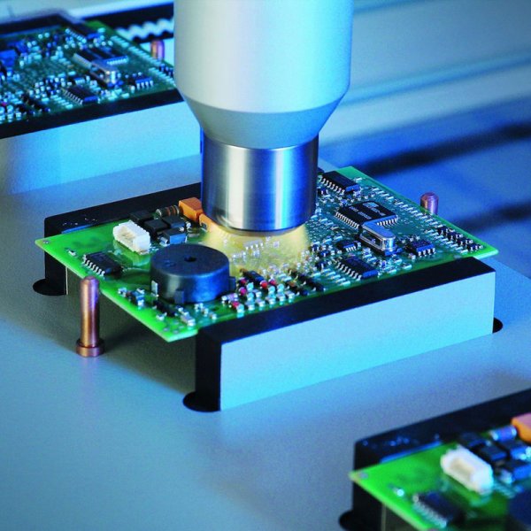
What is the application of plasma processing machines in the semiconductor industry? Let's take a look together.
1. Optimize wire bonding (wire bonding)
The product quality of integrated circuit chip wire bonding has a fundamental impact on the system reliability of microelectronic devices. The bonding area must be free of pollutants and have excellent bonding performance. The widespread presence of pollutants, such as oxides, organic chemical residues, etc., seriously weakens the tensile strength of wire bonding. Traditional wet cleaning does not completely or cannot remove pollutants in the bonding area, while the use of plasma cleaning can effectively remove the surface dirt of the bonding area and activate its surface, which can greatly increase the bonding tension of the wire and greatly improve the system reliability of the packaged device. Therefore, it is relatively better to use a plasma cleaning machine in the semiconductor industry.
2. Pre-treatment of power chip bonding
The bonding of power chip and packaging substrate is generally two types of materials with different properties. The surface of the material generally exhibits hydrophobic and inert properties, and its surface bonding performance is poor. Gaps are easily generated at the interface during the bonding process, which brings great hidden dangers to the power chip after sealing and packaging. Plasma treatment of the surface of the power chip and the packaging substrate can effectively increase its surface activity, greatly improve the fluidity of the bonding epoxy resin on its surface, enhance the bonding wettability of the power chip and the packaging substrate, reduce the stratification of the power chip and the substrate, improve the thermal conductivity, enhance the system reliability and stability of the IC package, and increase the life of the product.
In flip chip packaging, plasma treatment of power chips and packaging carriers can not only obtain an ultra-clean welding surface, but also greatly improve the activity of the welding surface, which can effectively prevent cold solder joints, reduce voids, and improve the reliability of welding systems. At the same time, it can increase the edge height and inclusiveness of the filler, improve the mechanical strength of the package, reduce the shear force formed at the interface due to the thermal expansion coefficients of different materials, and improve the reliability and life of the product system.
3. Surface treatment of lead frame
In the field of microelectronic packaging, the plastic packaging form of lead frame still accounts for more than 80%. It mainly uses copper alloy materials with excellent thermal conductivity, electrical conductivity and processing performance as lead frame. Copper oxide and some other organic chemical pollutants will cause the stratification of sealing molding and copper lead frame, resulting in poor sealing performance and chronic gas permeation after packaging. It will also affect the bonding and wire bonding product quality of power chip. Ensuring the ultra-cleanliness of lead frame is the key to ensuring the reliability and yield of packaging system. Plasma treatment can achieve the effect of ultra-purification and activation of lead frame surface, and the yield of finished product will be greatly improved compared with traditional wet cleaning.
4. Ceramic packaging
In ceramic packaging, metal slurry printed circuit board is generally used as bonding area and cover sealing area. Plasma cleaning can be used before electroplating Ni and Au on the surface of these materials to remove organic contamination and significantly improve the quality of the plated products.
COMPANY:Shenzhen Jietongtai Technology Co., Ltd
Contact:Mr. Zhou
Tel:13410974163
Phone:15338087819
Email:mail@jietongtai.com
Add:A3 Floor, Hongda Phase III Factory, No. 9-2 Xingye 3rd Road, Fenghuang Community, Fuyong Street, Bao'an District, Shenzhen