welcome To Shenzhen Jietongtai Technology Co., Ltd Official website!
语言选择:  |
|  |
| 
| | | | 
1. Application of plasma cleaning technology in circuit boards:
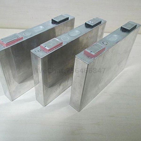
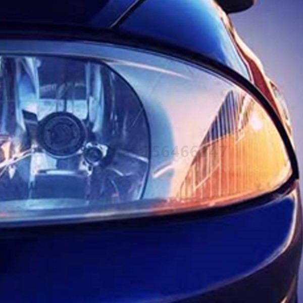
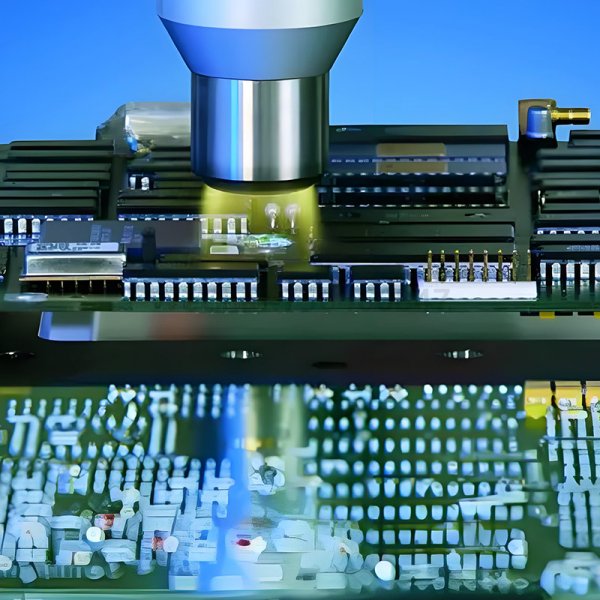
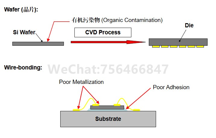
The plasma surface cleaning technology is now being used in various fields such as LCD, LED, IC, PCB, SMT, BGA, lead frame, and flat panel display cleaning and etching. Plasma-cleaned ICs can significantly improve the strength of wire bonding and reduce the probability of circuit failure; spilled epoxy resin, residual photoresist, solvent residues, and other organic pollutants can be eliminated in a short time after exposure to the plasma range.
PCB manufacturers use plasma cleaning machines to remove pollutants and remove insulation in drilled holes. For many new products, whether they are used in industrial production or electronics, international aviation, health and other fields, their reliability depends largely on the bonding strength between the two surfaces. Whether the surface is metal, ceramic, polymer, plastic or a composite thereof, the adhesion can be effectively improved after plasma treatment, thereby improving the quality of the final new product. Plasma cleaning is safe, environmentally friendly and economical in the process of improving the activity of the surface of any material.
2. Application scenarios of plasma cleaning in circuit boards
COMPANY:Shenzhen Jietongtai Technology Co., Ltd
Contact:Mr. Zhou
Tel:13410974163
Phone:15338087819
Email:mail@jietongtai.com
Add:A3 Floor, Hongda Phase III Factory, No. 9-2 Xingye 3rd Road, Fenghuang Community, Fuyong Street, Bao'an District, Shenzhen