welcome To Shenzhen Jietongtai Technology Co., Ltd Official website!
语言选择:  |
|  |
| 
| | | | 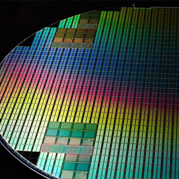
Plasma cleaning is driving a revolution in new developments in the semiconductor industry. It provides enhanced cleaning, surface modification and advanced etching processes. By utilizing ionized gases, this method not only removes contamination with incredible efficiency, but also controls surface conditions to improve adhesion.
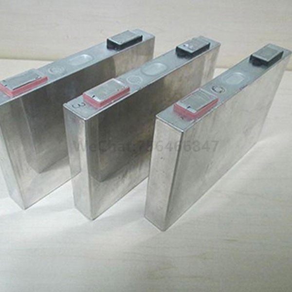
Main application processes of plasma cleaning technology in semiconductor packaging:
Flip chip
Use atmospheric pressure hydrogen and argon plasma to remove oxides from indium, tin and copper micro-bump arrays
Underfill
Activate the surface under the BGA, CSP or flip chip before dispensing the underfill
Wire bond
Remove organic contaminants from the bonding pads on the lead frame before wire bonding
Molding
Activate the lead frame and other packages for bonding before encapsulating the chip in the epoxy resin mold
Wafer hybrid bonding
Bonding)
Activate the glass film for direct melt bonding without adding any particles to the wafer surface
(1) Wafer cleaning:Remove residual photoresist
(2) Before packaging silver glue:Greatly improve the surface roughness and hydrophilicity of the workpiece, which is conducive to silver glue flattening and chip pasting. At the same time, it can greatly save the use of silver glue and reduce costs
(3) Cleaning before wire bonding:Clean the pad, improve welding conditions, and improve welding reliability and yield
(4) Plastic encapsulation:Improve the reliability of the bonding between the plastic encapsulation material and the product and reduce the risk of delamination
(5) Cleanliness of the lead frame:After microelectronic packaging, the sealing performance is prone to deterioration and chronic gas permeation, which will also affect the bonding and wire bonding quality of the chip. How to ensure the cleanliness of the lead frame is the key to ensuring packaging reliability and yield. After cleaning by plasma surface treatment machine, the surface purification and activation of lead frame will greatly improve the yield of finished products compared with traditional wet cleaning, and eliminate wastewater discharge, reducing the cost of purchasing chemical solutions.
(6) Quality of integrated circuit lead bond:It has a decisive influence on the reliability of microelectronic devices. The bonding area must be free of pollutants and have good bonding characteristics. The presence of pollutants, such as chlorides, organic residues, etc., will seriously weaken the tensile strength of the lead bond.
COMPANY:Shenzhen Jietongtai Technology Co., Ltd
Contact:Mr. Zhou
Tel:13410974163
Phone:15338087819
Email:mail@jietongtai.com
Add:A3 Floor, Hongda Phase III Factory, No. 9-2 Xingye 3rd Road, Fenghuang Community, Fuyong Street, Bao'an District, Shenzhen